While artifacts relating to the charge of MIBL lithography ions are often imperceptible, charging of masks, always contaminated by thin insulating films of polymerized vacuum oils, and insulating substrates can lead to fatal pattern transfer errors. Unlike substrate charging, ions deflected by mask charge results in resist exposures that are laterally displaced by an amount proportional to the proximity gap. Thus, mask charging is particularly important in large depth-of-field applications such as the fabrication of sensors and electronics over the steep topography of micromachined silicon wafers. It is also important for the fabrication of nanoscale planar features where the gap may be small, but their small size makes even the smallest deflection unacceptable. Examples are described in the following paragraphs.
Lithography on Insulating Substrates
We originally developed ABL as part of a larger ion projection lithography program, to study the distortion of large area stencil masks during ion exposure. These masks were fabricated with a 4 × 4 cm2 pattern area in a 3 μm thick silicon membrane, 12 cm in diameter. Figure 5b shows a metallization pattern with 0.7 μm minimum feature size. The plan was to copy the masks using IBL onto photomask plates with the same ion energy, 10 keV, as in the projector then under development. The distortion of the pattern on the photomask plates would then be measured with the standard metrology tools. We used a tri-layer resist scheme to amplify the rather thin (~0.1 μm thick) resist layers that could be accurately exposed with 10 keV ions. The resist stack is shown in Fig.5a. The resist coating supplied on the photomask plate was hard baked and sequentially coated with a 50 nm thick SiO2 pattern-transfer layer and a 100 nm thick film of Poly(methylmethacrylate) (PMMA) resist. After exposure and development, the PMMA pattern was transferred into the SiO2 by reactive ion etching in a CHF3 plasma (CHF3-RIE) and into the hard baked photoresist by O2-RIE. It was a surprise to find that, after MIBL exposure, the PMMA lines had the unusable, micron-scale line-edge roughness (LER) shown in Fig. 5c. Because large-scale roughness was entirely absent on conducting substrates with the same PMMA thickness, it was clear that the problem was that the ion range was too short to reach the chromium layer where the implanted charge could be conducted away. One option at this point was to use a conducting film to prevent substrate charging. A simpler approach emerged, however, by sweeping the ions out of the beam with electrostatic deflectors. A neutral particle contamination, constituting about 10% of the ion flux, however, was unaffected by the deflectors and exposed the resist, although with a significantly longer exposure time. As shown in Fig. 5d, line edge roughness was then entirely. Referring again to fig. 5a, implanted ions create an isolated, non-uniform charge distribution within about 170 nm (the range of the ions or neutral particles) of the surface. This charge build-up causes severe distortion of the ion beamlets during exposure. Secondary electron emission should create a similar charge distribution during neutral atom exposures, however, being neutral, they are immune to this charge. Thus, the use of neutral particles instead of ions to copy the stencil masks provided a simple and complete solution to the charging problem of IBL on these insulating substrates.
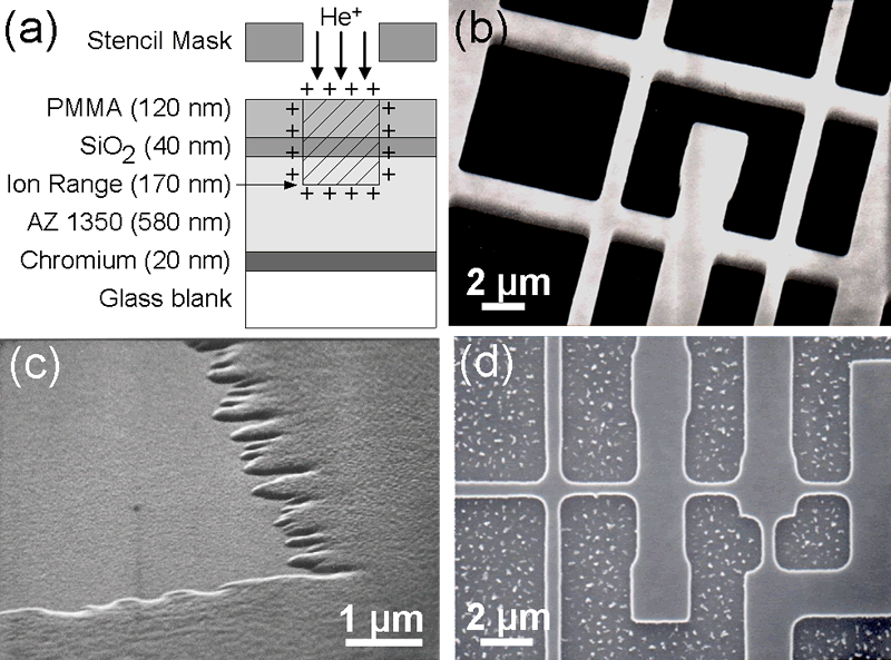
Figure 5: (a) Sketch of the tri-layer lithography experiment. SEM images of (b) representative structures in the silicon stencil mask, (c) micron-scale, line-edge roughness due to substrate charging in IBL exposures, and (d) the crisp image, etched through to the Cr layer, when the mask is exposed by neutral He atoms instead of ions.
Mask Charging: Large Proximity Gaps
Helium ion and neutral particle exposures were performed at large proximity gaps on a conducting silicon substrate with a 100 nm thick layer of PMMA and a nominally conducting 1.0 μm thick silicon mask with a 3.6 × 3.6 cm2 pattern area. Since the resist is thin and its surface is discharged to the substrate by particle-induced conductivity, there are no artifacts due to substrate charging. The ABL images are shown in Figure 6 a and 6b for proximity gaps of 80 μm and 1.13 mm, respectively. Despite the large variation in gap, the two images appear remarkably similar and have near identical values of LER, as measured along a 1 μm long edge centered on the arrows in (6a). However, in the MIBL images, 6c and 6d with proximity gaps of 0.60 mm and 1.13 mm, an additional component of excess LER is readily apparent, increasing by 8.1 and 15.6 nm (3σ), respectively, relative to that of 6a and b. Figure 7 shows MIBL excess LER versus proximity gap. Clearly, excess LER is proportional to proximity gap and due to deflection of the beamlets as they pass through this mask. The qualitative similarity between the roughness in the ion and neutral atom images suggests that specific sites on the mask are charging, even though many are too small to be resolved in the neutral particle image. Clearly, eliminating these insulating regions would require a considerable development effort. Even if the mask were initially conducting, polymeric contamination during use would shorten its life as an ion mask. ABL, on the other hand, is immune to the presence of insulating regions in the mask.
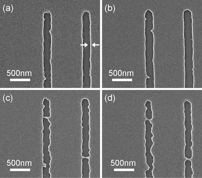
Figure 6: SEM images of the same mask feature printed with ABL at mask-to-substrate gaps of (a) 80 μm and (b) 1.13 mm and with MIBL at gaps of (c) 0.60 mm and (d) 1.13 mm.
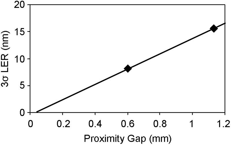
Figure 7: Excess line edge roughness in ion beam lithography as a function of proximity gap.
Mask Charging: Nanoscale Features with Small Proximity Gaps
Mask charging artifacts can also be seen when printing nanoscale structures even with a very small proximity gap. Figure 8a shows a 100 x 400 nm fish-shaped defect in a 500 nm wide line in a 3.0 μm thick silicon mask with a 0.6 μm thick diamond-like carbon (DLC) ion absorbing layer. A 2 nm thick iridium coating was applied to prevent gross charging of the DLC during ion exposures. The mask was printed with 30 keV He+ ions and neutral atoms in 50 nm thick PMMA over 20 nm thick thermal oxide on a silicon substrate. There should be sufficient particle-induced conductivity to prevent substrate charging. Exposures were carried out at twice the critical dose with a 20 μm proximity gap, corresponding to a penumbral blur of only 0.8 nm. After development, the resist pattern was transferred into the SiO2 to a depth of 10 nm by CHF3-RIE and the remaining resist removed in an O2 plasma. SEM imaging was done with a beam energy of 20 keV directly on the oxide pattern. SEM charging artifacts are absent with this ultra-thin oxide. The mask appears to be perfectly smooth at the nanometer scale. The ABL image in Fig. 8b shows very fine ripples (label A), which correspond to a roughness of about 6 nm (peak-to-peak). This rippling, which must be due to slight protrusions on the mask sidewalls, is amplified, point-by-point, to about 15 nm in the ion image shown in Fig. 8c. Enhanced roughness is also seen on the lower edge (label B) of the line in the MIBL image that can, in some cases, be mapped to roughness in the ABL image.
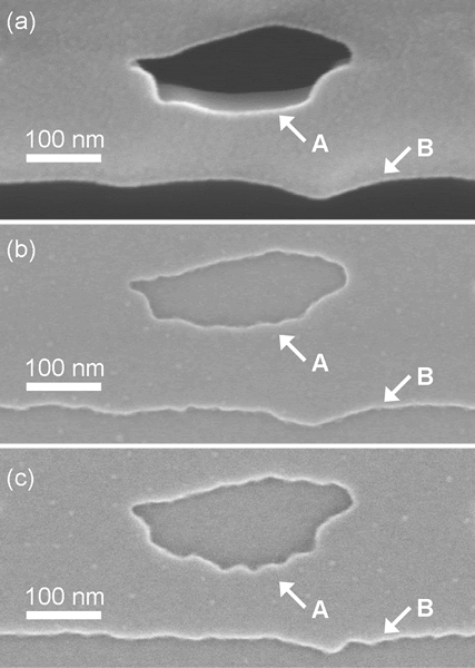
Figure 8: SEM images of (a) a fish-shaped mask and corresponding (b) ABL and (c) MIBL images etched into SiO2.
Figure 9 (a) shows a 13 nm wide mask feature and the secondary electron signal along a line across this feature. Linewidth has been defined, somewhat arbitrarily, as the distance between the brightest points in the image. The ABL print in (b), transferred into the SiO2 as above, has a similar shape and a corresponding linewidth of 15 nm; a pattern fidelity of 2 nm for the 13 nm feature. This widening corresponds to the accepted ~1 nm range of secondary electrons in PMMA resist.
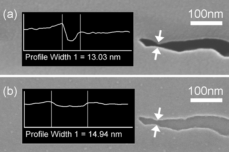
Figure 9: SEM images of (a) a 13 nm wide mask feature and corresponding (b) ABL image etched into SiO2. Insets show the secondary electron profile along a line between the arrows.
Mask Technology
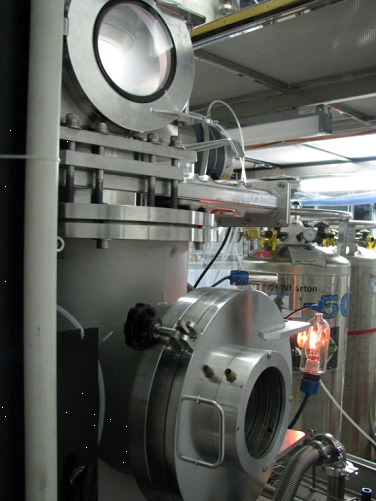
As discussed above mask fabrication is an essential component of both MIBL and ABL. The most advanced mask technology, which we have used since 1986, is based on silicon membrane technology now widely available in the MEMS community. Etching transmission windows in silicon membranes uses bromine based (Br2 or HBr)-RIE which we showed to be intrinsically anisotropic even for heavily doped n-type membranes. The current incarnation of the etching process uses a dual chamber, magnetically enhanced etching tool, largely built by Dr. Ananya Roy to support her Ph.D. research. The reason for 2 chambers is that one can be dedicated to etching the SiO2 hard mask with C4F8 while the other is maintained in pristine condition for etching silicon, which is very sensitive to contamination. The tool is shown in Fig. 10a. Dr. Roy is shown with the tool in 10b. Figures 11a and 11b shows a mask used to fabricate GPS SAW filter in the 1990s. Figure 12 shows an array of high quality 75 nm transmission windows etched in Dr. Roy’s etching tool, Fig. 10 a, b.
(a)

(b)
Figure 10: (a) Dual chamber mask etching tool and (b) Dr. Roy who built the tool to support her dissertation research.
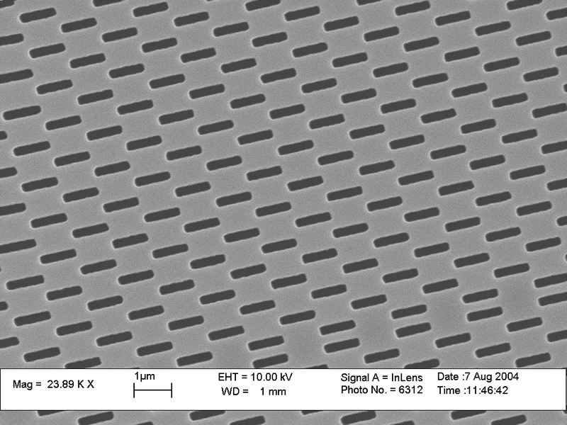
Figure 11a: Silicon stencil mask used for fabricating 0.25 µm interdigitated electrodes in 2 offset exposures. This mask was used to fabricate surface acoustic wave filters for GPS (ca 1993), a project supported by Motorola
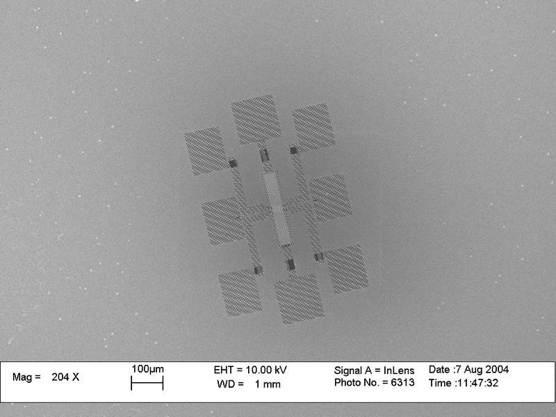
Figure 11b: Birds-eye view of a 0.9x1.4 mm2 SAW mask including the bonding pads. The high density structures in the center of the device is the active area of the filter shown in Fig. 11a.
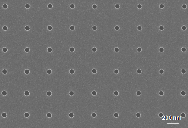
Figure 12: Micrograph of a silicon stencil mask with high quality 75 nm transmission windows that was fabricated in the dual chamber etching system.
Plasma Enhanced Chemical Vapour Deposited (PECVD) Resist
As discussed above, a very small source size and the absence of diffraction provides Chrysalis with an enormous depth of field. To realize this potential for 3-D circuit topography requires a conformal resist deposition process. To fill this need we have developed plasma enhanced deposition (PECVD) process with styrene feed stock. The reactor is shown in Figure 13. The sample is attached to a window about 10 cm from a hollow, RF-driven (13.56 MHz) aluminum cathode, which contains a ferrite magnet polarized normal to the cathode face. An external counter-magnet behind the sample, polarized in the same direction as that of the cathode, creates a ~ 25 Gauss magnetic field that traps cathode electrons, forming an electron beam that polymerizes adsorbed monomer on the substrate. The area of the cathode facing the sample is 50 cm2. No carrier gas is used. Under suitable conditions, the deposit is soluble in amyl acetate but exposure to 30-75 keV helium ions or atoms results in a durable, cross-linked coating that is insoluble in organic solvent, even concentrated inorganic acids at room temperature. When used as a resist, its sensitivity and contrast are 30 µC/cm2 and 3, respectively. A rotary fixture can be used for coating 3-D substrates, such as optical fibers. Currently, the resist deposition rate is 20 nm/minute. Figure 14 shows four 15 µm wide resist lines on the sides of a 2.5" optical fiber 60 mm in diameter. A special micromachined jig was used to align the mask with the fiber.
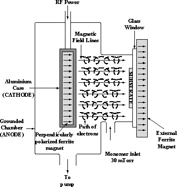
Figure 13: Magnet plasma enhance chemical vapor deposition system for conformal resist coatings.
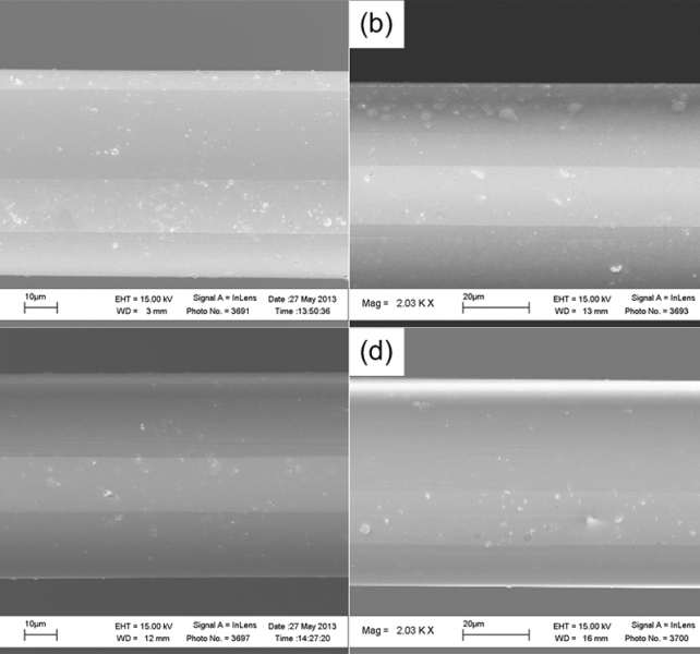
Figure 14: (a)-(d) Four 15 µm wide gold conductor lines for recording signals in the brain on a 2.5" long optical fiber fabricated by Chrysalis using plasma deposited resist. The fiber was aligned using a special V-groove jig.
Protective Mask Coatings
Ion damage to the mask is a significant issue. Currently, the backside is protected with a coating of nanoporous diamond-like carbon (DLC), which absorbs lithography ions with little change in stress. It is deposited by PECVD in a parallel plate system, after which, the mask pattern is transferred to the DLC by O2-RIE. Figure 15, which shows the backside of a DLC-coated silicon mask, demonstrates the ability to transfer ~10 nm striations in the silicon masks faithfully into the DLC.
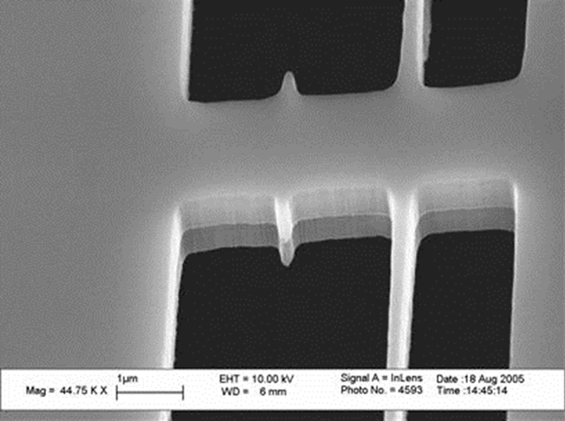
Figure 15: A 370 nm thick protective coating on a 400 nm thick silicon stencil mask. Note the replication of nanoscale roughness from the silicon mask into the film, and the absence of undercutting.