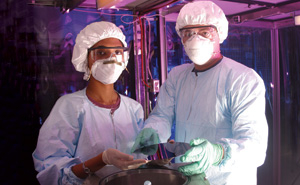
The mission of the Nanosystem Manufacturing Center is to develop technology for manufacturing integrated nanosystems. Support from the National Science Foundation in 2008 continued the development of an advanced neutral beam printer and supporting mask-making hardware for a high throughput lithograph in the sub-100 nm regime. Other projects by these center researchers include a proof of concept tool for removing photoresist from 300 mm silicon wafers through a collaboration with Axcelis Technologies Inc., as well as the development of two new concepts for fabricating water filters that are currently being evaluated by potential investors. Researchers also demonstrated, for the first time, the ability to fabricate nanoscale structures in 3-D. Among the main accomplishments of the center:
- Neutral beam lithography: This is a proximity printing technique where a stencil mask (a membrane with open transmission windows) is flooded by a broad beam of energetic (e.g. 30 keV) helium atoms and transmitted beamlets expose resist on a substrate. The major accomplishments last year included a careful study of the advantages of this technique vis-Ã -vis ion beam proximity lithography, the development of a mechanical nanostepping capability with sub-nanometer pattern placement accuracy, and the development of advanced source technology. Our work is summarized in an invited review article in Journal of Physics D (Jan.-Feb., 2008).
- Photoresist ashing: Resist masks are used in every level of integrated circuit manufacturing. We solved the long standing residue problem in ashing high dose, ion implanted photoresist, thus eliminating several expensive cleaning cycles in integrated circuit manufacturing. Because of this advance, we were contracted by Axcelis Technologies Inc. to build a proof-of-concept tool for ashing 300 mm silicon wafers. The tool is now undergoing shake-down tests before starting an evaluation program with several major integrated circuit chip manufacturing companies. Through this project, we developed a new way to measure substrate loss during resist ashing in collaboration with Axcelis and Professor Wolfgang Donner in the department of physics. The approach has unprecedented accuracy—about 0.5 angstroms or just 1/4 of an atomic layer.
- 3-D lithography: A novel plasma enhanced resist coating process was developed with NSF sponsorship that unlocks the potential of ion and neutral beam proximity lithography for patterning 3-D surfaces. The technique is expected to find wide application in microelectromechanical systems (MEMS). The technique enabled the fabrication of multichannel cuff electrodes about 10 times smaller than what exists today. We used the cuffs to monitor neuronal signals in a grasshopper. This research is part of a larger program with Professor Richard Liu the UH Department of Electrical and Computer Engineering and Professor Fabrizio Gabianni in the Neuroscience Department at the Baylor College of Medicine. Profs. John A. Dani, Gopathy Purushothman, Weichuan Shih, and Jack Wolfe have applied the technology to fabricate neural probes with integrated conductor wiring on ultra-thin optical fibers that provide significantly better localization of neuronal signals and displace 90% less brain tissue than state-of-the-art competitors. The probes are being used to map neural circuits in the brain.
The Center’s core facility contains a suite of unique nanomanufacturing tools, including 1) a large area, high throughput, neutral particle printer with sub-nanometer resolution, 2) a large area plasma enhanced chemical vapor deposition tool for conformal resist deposition on aggressive 3-D topography, 3) a dual chamber reactive ion etching system with F, Cl, and Br chemistries for etching silicon, SiO2, tungsten, and a variety of other materials, 4) a 3-gun sputter coater, and 5) an ion-enhanced electron-beam deposition system. It also has a small clean room with acid and solvent decks, a resist spinner, a Kasper contact printer, two 4” Minibrute tube furnaces, and a 6” rapid thermal processor. NMC also has access to a research grade scanning electron microscope in the Engineering Microscopy Center and the facilities of the University of Houston’s clean room facility.
The Center currently supports active research in 1) particulate filter manufacturing, 2) bio-microelectromechanical systems (BioMEMs), 3) surface and intravascular probes for magnetic resonance imaging, 4) applications of nanomaterials to water treatment and the prevention of biocorrosion, 4) nanobiophotonics, 5) neural probes for deep brain stimulation and recording, 6) plasmonic engineering, 7) nanobiophotonics, and 8) hyperspectral imaging.
The Center is engaged in active research collaborations with Methodist Hospital (Houston), the University of Pennsylvania, the Vanderbilt University School of Medicine, and three small businesses.
The center has 18 Ph.D. and 28 M.S. graduates. Three women received degrees from the program; Dr. Mansi Bhargava (plasma jet development and metrology) & Dr. Manwen Yao (biosensors), and Ms. Dhara Parikh, who received an MS degree for her work in 3-dimensional lithography. The Center is poised to play a critical role in UH’s strategic plan as the health-care and energy focus areas evolve.